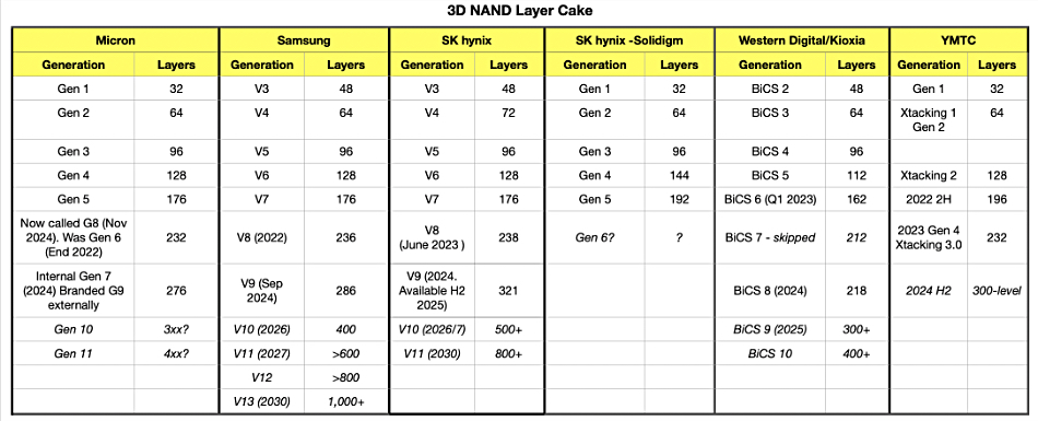
Samsung, currently on its ninth-generation 3D NAND with 286 layers, has 400-layer technology in development. This was revealed via a 2025 IEEE International Solid-State Circuits Conference agenda release [PDF]. Session 30.1 on February 19, page 65, is titled “A 28Gb/mm2 4XX-Layer 1Tb 3b/cell WF-Bonding 3D-NAND Flash with 5.6Gb/s/pin IOs” with a paper written by a Samsung team. This 1 terabit NAND chip has a 28 Gb/mm2 density, 400-plus layers, and a triple-level cell (3b) format, and will be Samsung’s tenth generation of its V-NAND technology. Gen 9 chips have two-string stacking, with 2 x 143 decks, and come in both TLC and QLC (4bits/cell) formats. Gen 9 V-NAND supports data speeds up to 3.2 Gbps whereas the new 400-plus-layer technology supports 5.6 Gbps per pin, 75 percent faster. That speed seems suited to both PCIe 5 and the twice-as-fast PCIe 6 interconnects. “WF-Bonding” refers to wafer-to-wafer bonding, in which two separate NAND wafers, on which cells and/or circuits have been fabricated, are attached to each other. Such bonding enables each wafer’s fabrication process to be optimized in terms of scalability, performance, and yield.

The highest in-production layer counts are SK hynix with 321, followed by Samsung with 286, and Micron with 276. Western Digital and Kioxia’s BiCS process has 218 layers with a 300-plus-layer BiCS 9 generation in development. SK hynix’s Solidigm subsidiary is back in the layer count dark ages, so to speak, with its 192-layer technology in QLC format, notwithstanding that it just announced a high-capacity 122 TB SSD using this 3D NAND. China’s YMTC has a 300-layer chip coming.
We know some storage suppliers have been discussing 256 TB drives and assume these will use more advanced layer counts than are currently available. Samsung has its existing QLC BM1743 SSD with 61.44 TB capacity built from 176 layers; its seventh-generation V-NAND. With Samsung V9’s 286 layers and V10’s 400+layers, higher capacities such as 256 TB and even 512 TB become possible, as well as higher-capacity embedded SSDs used in smartphones, vehicle ADAS systems, and the like.
We don’t know if and when a Samsung 400-plus-layer NAND chip will enter production. That will be a decision for its new management.


 中文 (中国)
 Русский